Semiconductor nanostructures analysis
Advancing nanoscale II-VI semiconductors for better optical properties and improved device performance.

The project investigated the controlled synthesis and optical properties of II-VI semiconductor nanostructures, focusing on zinc and cadmium chalcogenides. These materials possess direct band gaps and high fluorescence yields, making them suitable for applications in LEDs and photodetectors. However, limitations in current wafer fabrication methods hinder practical use. By employing nanotechnology, the project significantly enhanced optical properties and reduces defect densities. It also examined the integration of diverse chemical compositions into hierarchical nanostructures and explored controllable doping to tailor optical characteristics. Results indicated substantial improvements in photocurrent and photoluminescence, with CdS nanoribbons demonstrating a conductance increase by four orders of magnitude and faster photoresponse times compared to conventional films. These advancements underscored the potential of II-VI semiconductor nanostructures for developing high-sensitivity and high-speed nanoscale devices, suggesting their promise for future optoelectronic technologies.
-

Original project funded for three years from 2004
Key topics
- Semiconductor nanostructures
- II-VI semiconductors
- Colloidal synthesis
Directors
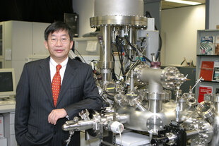
Shuit Tong Lee
Director at the City University of Hong Kong

Xiaohong Zhang
Professor at Chinese Academy of Sciences


Other projects

Adult stem cell regeneration
Original project funded for three years from 2024

Chiral electronic materials
Original project funded for three years from 2024

Glioma drug resistance
Original project funded for three years from 2024

Treg heart regeneration
Original project funded for three years from 2024
Stay in the loop!
Subscribe to keep up with the latest from Croucher Foundation.